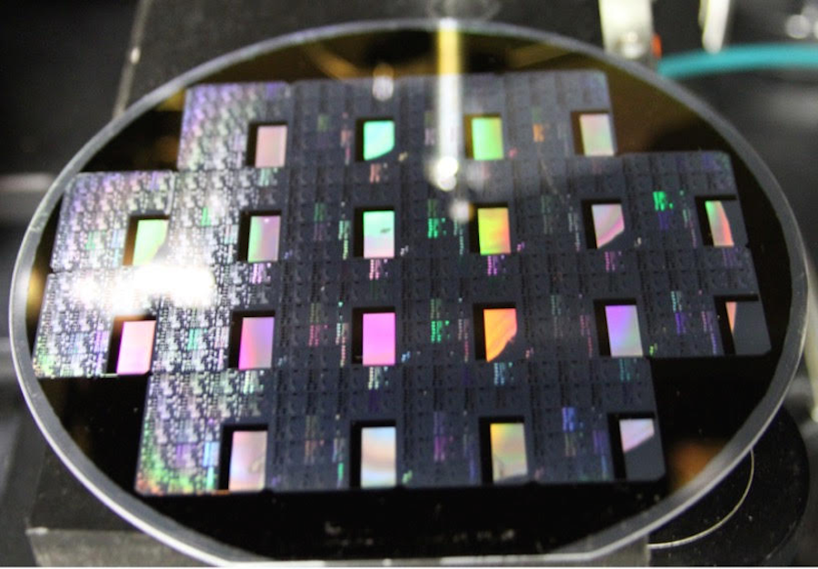
Innovative silicon wafer technology serves as game-changer for high speed connections at data centers
The immense growth of data centers powering the internet cloud has brought with it a demand to move large quantities of data faster and farther. Newly developed silicon wafer technology with tiny black holes, developed by UC Davis electrical engineers, acts a photodetector to move massive amounts of data worldwide at a cheaper cost.
Saif Islam of the UC Davis Department of Electrical and Computer Engineering collaborated with the Silicon Valley startup company W&W Sens Devices Inc., to develop this technology. The research was recently published in the online journal, Nature Photonics.
“Big data is what everyone talks about these days,” said Yang Gao, a postdoctoral scholar in Islam’s group. “The need for faster optical communication and the demand for higher bandwidth cloud computing are growing exponentially.”
The eminent “cloud,” is a metaphor for the internet. Cloud computing means storing and accessing information and programs over the internet instead of on a computer hard drive.
The main application of new silicon wafer technology is for data centers. A central issue of optics for data communication in the centers is the expensive cost for the data transfer rate, which is currently about $10 per gigabit per second.
“We believe this technology will help to further reduce the cost to single digit dollar per Gb/s,” said postdoctoral scholar Hilal Cansizoglu of the UC Davis Integrated Nanodevices and Nanosystems Lab.
The most striking feature of this new technology is the pattern of tiny black holes tapered in the silicon, only about 1 micrometer in size.
These holes essentially trap photons, which are tiny quantized particles of light, and divert them sideways which allows for high-speed data connections.
“A large number of simulations, experimental attempts and combined approaches helped us narrow-down our design window [for the optimal pattern of tapered holes],” Islam said.
After two long years of experimentation, the researchers concluded on a pattern of holes that taper toward the bottom of the wafer.
Traditionally, silicon is not considered a good material for a photodetector to use in data communication applications because very thick layers are needed to absorb light efficiently. Thick layers prevent the detector from having a fast speed and therefore produce a low data transmission. However, the new silicon wafer technology simultaneously has features of high data collection efficiency and high data transmission rate.
“Our designs use very thin silicon layers with photon-trapping holes, and the light coming into the photodetector is bent sideways so that it can be absorbed efficiently,” Gao said. “At the same time, the thin active region results in the data conversion rate of 25 gigabits per second and higher.”
Currently, when computer engineers want to move large quantities of data at a fast rate, the use of fiber-optic cables are employed. These cables transmit the data as pulses of light, and at the receiving end of the transmission is a detector that converts these signals to electronic pulses.
Unfortunately, in order to capture the all the data and be efficient as possible, the downside is a slow rate. In these situations, materials such as gallium arsenide can be used to increase speed and efficiency about, 10 times more, but it is significantly more expensive.
“This new [silicon wafer] technology [with tapered holes] and many others can make the optical communication more affordable, more efficient and ultimately improves the user experience that benefits everyone,” Gao said.
The ability for electrical engineers at UC Davis to collaborate with other engineers and scientists both within the UC system and other laboratories has contributed to the success of an experimental photodetector and solar cell using the new technology.
“UC Davis is luckily backed by a wide spectrum of available microfabrication tools and facilities both at Davis and in UC system,” Gao said. “We have access to several of national leading nanofabrication research facilities including Center of Nano-MicroManufacturing (CNM2) at UC Davis, and Marvell Nanofabrication Laboratory at UC Berkeley.”
High speed connections are increasingly vital at data centers, and the silicon wafer technology can be a game changer for how data is transmitted.
“The publication of this technological breakthrough has the potential to spark new design ideas and impact academic and industrial research toward the development of higher efficiency photodetectors,” Gao said.
Written by: Shivani Kamal — science@theaggie.org


